
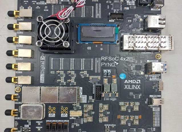
The VLSI Design and Test Labs should be presented as one of ESE’s core enabling academic and research infrastructures. These labs support digital, mixed-signal, memory, hardware-security, AI-hardware, cryptographic, and architecture-oriented work across simulation, design entry, verification, FPGA-based system prototyping, and chip bring-up.
The page should highlight that the lab ecosystem supports both coursework and advanced research. This includes CAD environments, servers and compute support, FPGA platforms, measurement and debug equipment, ASIC characterization setups, and system prototyping infrastructure. The narrative should also reflect the department’s growing capability in chip implementation and validation, not just design-only workflows.
Representative functional categories may include: digital design and verification environments; FPGA prototyping platforms; mixed-signal and memory testing support; ASIC characterization setups; hardware-security evaluation support; and training infrastructure used in advanced VLSI and system-design courses.